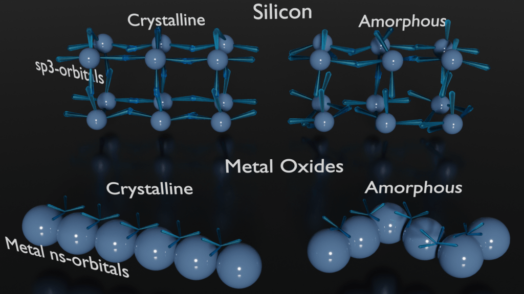
Metal-oxides (MOs) are wide bandgap semiconductors that can be solution-deposited using scalable coating techniques. After coating and subsequent thin-film formation, an annealing step (~300 °C) converts the precursors into the MO lattice. When used as channels in a field-effect-transistor (FET), these materials usually show n-type charge transport. Electron mobilities are significantly higher than amorphous Si and can be >10 cm2V-1s-1. In this family, Indium Oxide (In2O3) stands out given the ease of oxygen-vacancy formation responsible for high free electron densities that can fill traps and result in high electron mobilities. From an atomistic/orbital picture, MOs can withstand more mechanical strain without compromise on their charge transport properties, compared to Si (Figure 1). This makes MOs attractive for flexible electronics applications – large-area displays and wearable electronics – given the potential to scalably coat them at low-processing temperatures using industrially-relevant techniques such as slot-die, blade-, and spray-coating.
Figure 1. MOs vs Si: ns-orbitals in MOs allow for mechanical deformation (flexibility) without compromise on charge transport, unlike Si where twisting of sp3 orbitals results in disorder and significantly compromised charge transport.
NIST Highlight: Above the atomistic picture, exists the ‘mesoscopic’ picture. The precise manner in which MO lattices come together to form crystalline MO domains also dictates charge transport. Figure 2 is a highlight of my research work on MO electronics done while I was a postdoctoral researcher at NIST. Controlled coating resulted in highly textured domains aligned parallel to the substrate, as evidenced by Grazing-Incidence X-ray Scattering (GIXS) measurements performed at the Complex Materials Scattering (CMS) beamline of NSLS-II. These led to remarkably flat films (surface roughness ~0.1 nm) and electron mobilities approaching 20 cm2V-1s-1, at par with vacuum-deposited oxide electronics. In contrast, randomly-oriented disordered domains hampered transport and mobilities of only 5 cm2V-1s-1 could be realized.
The top interface of these ultrathin films behaves as a ‘sensor’ given its close proximity to the underlying gate dielectric. It should be noted that such thin (low-dimensional) systems have a high surface-to-volume ratio similar to QDs, and passivation can help. We found that placing another ultrathin MO layer atop this surprisingly doubled the charge carrier mobilities (40 cm2V-1s-1) and the films exhibited band-like charge transport. We believe this is because the interfacial traps are now ‘buried’. This ‘double-coat’ does have its own interfacial traps at the top interface, but this interface is now farther away from the gate dielectric, meaning these defects states might not contribute to charge transport. Read the research article here. I also wrote an introductory blog piece for the Materials Research Society (MRS) on solution-processed MO electronics.
Figure 2. Microstructure plays a key role in printed electronics. Printing conditions can be tuned to manipulate microstructure, directly impacting electronic properties.
The ability to controllably coat MO inks at scale opens exciting opportunities in ‘film-engineering’. Imagine building up heterostructures of MOs – dissimilar MOs with differing band structures – that can have a and structure kink at the interface. For example, coating ZnO atop In2O3. Given its higher electronic concentration, electrons from In2O3 can populate and get localized in this interfacial kink. The result will be a localized 2D electron gas at the interface of the two oxide layers which can be gated. This can lead to exotic quantum phenomenon. Obviously, this physics is well-known and has been extensively explored in the past, but all that has required carefully grown crystals in high-purity environments. MOs inks present a unique opportunity to decentralize quantum electronics!